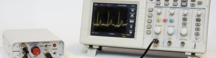
New non-invasive methods of monitoring the electrical behaviour of materials and devices are always of interest. EP sensors may be configured to measure either; potential, electric field or surface charge. This versatility enables a range of physical parameters to be accessed including; conductivity, dielectric constant and charge density. The scalable nature of the sensors means that we are able to miniaturise the measurement tip down to the order of one micron. The challenge has been to do this while still retaining the physically robust nature of the sensor. We have now achieved this with a 5 micron diameter sensor, enabling us to image with this resolution. The applications for this imaging system range from inspection of integrated circuits to forensics and the non-destructive testing of insulating (plastic) and composite (carbon fibre) materials.
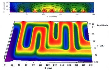 Image of signal in active integrated circuit, showing contours of constant potential above the surface
Our research aim is to build on this proof of principle demonstration using a single sensor and move towards one and two dimensional imaging arrays, with the same spatial resolution. A two dimensional array would enable real-time imaging of the electrical behaviour of a sample or device to be achieved over the whole of the active area of the imaging array.
For further information regarding this research, please contact Professor Robert Prance.