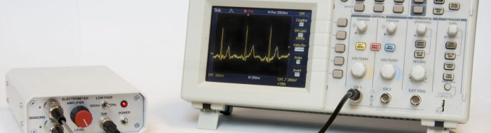
One particular example of a novel measurement instrument based on the microscopic version of the EP sensor has recently been applied to imaging the surface charge deposited by a finger when touching a plastic surface.
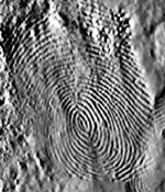 Charge image of fingerprint
This is a notoriously difficult scenario for conventional fingerprinting methods, with some materials, such as PTFE, being particularly challenging. Traditionally such a fingerprint would require chemical treatment to render it optically visible, thereby eliminating the possibility of subsequent DNA analysis. By contrast, EP sensors can image the fingerprint non-invasively without any treatment at high spatial resolution. In addition, because the surface charge decays in a well defined manner, dependent on the material and the humidity, it is possible to estimate when the fingerprint was deposited. This is not currently possible using existing techniques and would prove an extremely valuable tool to forensic investigators.
This ability to image surface charge on insulating materials is also of interest to the semiconductor industry, as a non-invasive inspection technique for use during the manufacture and testing of ICs and VLSI chips. The non-contact nature of the sensors is of particular importance here, where it offers the ability to image charge distributions beneath the inert passivation layer.
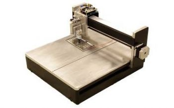 EPS scanning microscope
Our research aim is to build on this initial work using a single raster scanned sensor and to integrate many sensors into one and two dimensional arrays, which will allow much faster or real-time imaging to be achieved. In principle a two dimensional imaging array could be used by a scene of crime officer to assess rapidly which fingerprints were recent and should therefore be the focus of their investigations.
For further information regarding this research, please contact Professor Robert Prance.