A modular approach to quantum computing
In order to solve some of the most interesting real life problems using quantum computers, millions or even billions qubits may be required. It is impossible to accommodate so many quantum bits on a single quantum computing chip or module. Quantum computers therefore need to be modular in order to allow for sufficiently many qubits. There are two approaches to make a trapped ion quantum computer modular.
The most well-known approach makes use of photonic interconnects. Optical fibres are used to connect quantum computing modules. Coincident detection of photons on photodetectors results in the entanglement of two ions located on different quantum computing modules. This approach has been developed for over 15 years, however, because of the extreme technical difficulty with this approach, coupling rates between modules have been limited to values on the order of 10s per second after the required entanglement distillation is carried out. This seems far too slow to build practical quantum computers.
We have developed an alternative approach to modularity. Rather than using photonic interconnects, we use electric fields to connect quantum computing modules.
Adjacent quantum computing modules are aligned with an accuracy of approximately 10 micrometers. The electrodes on the edge of each quantum computing module are shaped such that the electric field lines connect in such a way that ions can be simply transported from one module to the adjacent one by applying appropriate voltages to the electrodes located on the edge of each quantum computing module. An artistic visualisation of this process is shown in Figure 1. This method is expected to provide for connection speeds up to 10,000 times faster than making use of photonic interconnects. More importantly, this approach allows for much simpler engineering to be used. Relaxing the engineering complexity is particularly important when working towards the development of quantum computers with millions of qubits.
![]()
We have developed an experiment to demonstrate this new approach to modularity. In this experiment many of the key features necessary for the construction of a multi-module quantum computer are incorporated. In particular, we will work on demonstrating ion transport between adjacent modules as well as demonstrating entanglement swapping between modules.
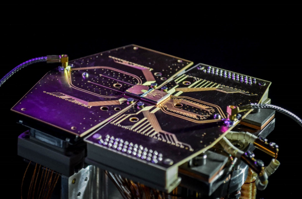
Figure 2: A picture of the experimental prototype setup for module to module shuttling of an ion qubit on two distinct surface traps. One the left side ion trap, the reflection of the light on the DC electrode clearly shows the distinctive pattern of a linear trap while an x-junction can be seen on the right hand side ion microchip.
To allow for ions to be physically transported from one module to another module, reasonable alignment between adjacent ion trapping modules needs to be accomplished. A depiction of the two-module prototype where two ion trapping modules are closely aligned is shown in Figure 2.
We have developed techniques to produce ion microchips with appropriate edges. We have demonstrated to create an edge with a surface flatness < 1 µm. The picture of a precisely microfabricated edge microchip is shown in Figure 3.
Using ultra-high vacuum compatible piezo actuators we can control the separation of the two ion microchips with resolution of < 0.1 µm. The experimental apparatus allows to investigate configurations with separations as large as 600 µm.
This approach is highly scalable, meaning once it is demonstrated with two modules and these modules can be fabricated reproducibly, then it should be possible build quantum computers with, in principle, any number of quantum computing modules, enabling quantum computing with an arbitrary number of qubits.
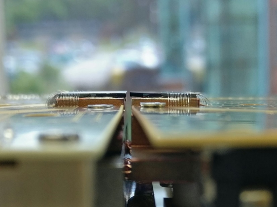
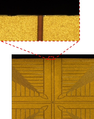
Figure 3: (Left) Rough manual alignment of two surface ion traps prior their installation in the vacuum system. The chips are intentionally left with a misalignment of ~200 µm to accommodate for material deformation during the baking of the vacuum system and cooling of the ion traps. (Right) Microscope picture of the ion trap edge after chemical etching of its border. The realisation of the well-defined edge allows for the precise alignment of the ion traps.
We also integrate ion shuttling within an x-junction into this prototype building on the expertise developed in other quantum computer prototypes here at Sussex. This allows for the demonstration of variable connectivity on a qubit ensemble where any two pair of qubits can interact with each other. This is another crucial step towards executing complex quantum algorithms.
Demonstrating a modular quantum computing approach where ion qubits are shuttled between ion trap modules should be demonstrated alongside an equally scalable entanglement generation scheme.
Alongside other quantum computing prototypes within the group, we implement a laser-free quantum gate approach, quantum computing with global radiation fields, which allows for the execution of quantum gates by applying voltages to an ion microchip.
Here, as with other experiments in the research group, we generate entanglement between the internal state of two ion qubits using local static magnetic field gradients and long-wavelength radiation fields. To deliver the global microwave fields, we use a patch antenna, which is directly mounted inside the vacuum chamber. To generate the local magnetic field gradient in a scalable manner, optimally designed current carrying structures are integrated within the ion trap substrate and can sustain current densities exceeding 106 A/cm2. There, the proximity between the embedded current carrying structures and the trap electrodes allow for gradients approaching 185 T/m to be generated at the location of the trapped ions. The drawing of a cross-section of the ion trap and SEM picture of the trap electrode is shown in Figure 4.
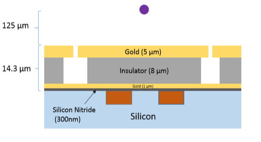
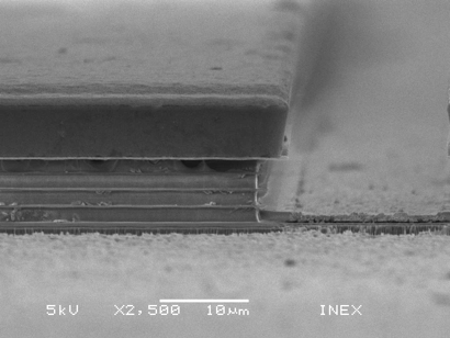
Figure 4: (Left) Cross-section drawing of a surface ion trap used in the prototype experiment. Current carrying structures integrated within the substrate are shown in orange, the ion is shown as a purple dot (the picture is not to scale). (Right) Scanning Electron Microscope picture of a gold electrode resting on an insulator stack in the microfabricated ion trap.
To generate entanglement between qubits, a pair of ions is shuttled to the gate location using a sequence of voltages applied to the trap electrodes. Then, turning on the current in the current carrying wire will bring the ion internal electronic states in resonance with the global radiation fields. This will allow for the specific addressing of this pair of ions and the realisation of an entangling gate with these particular ions. In accordance with our vision for the construction of a universal quantum computer module, this entangling zone is located in one of the arms of the x-junction ion trap, while ion loading and state detection can be realised in the other arms.
One key condition which helps achieve greater entangling gate fidelities is the operation of an ion trap at low temperatures. Indeed, given the required coupling between the ion internal qubit state to the collective motion of the ion pair during entanglement, the quality of the resulting entanglement is highly sensitive to a phenomenon, referred to as motional heating. Reducing the temperature of the trapping electrode below 100K has been found to significantly reduce motional heating by multiple orders of magnitude. In addition, operating at cryogenic temperatures close to ~50 K allows to take advantage of the improved electrical properties of conductors and enhanced thermal conductivity of the silicon substrate of the ion trap chip, enabling greater currents to be delivered to the trap and in turn greater magnetic field gradients to be generated at the ion location.
Under these conditions we anticipate that operating this ion trap setup at cryogenic temperatures will lead to two qubit gate fidelities exceeding the 99% fault-tolerant threshold for error correction using surface codes.
To cool both ion trapping modules down to cryogenic temperatures, we have developed a dedicated in-vacuum helium heatsink in which cold pressurised helium gas is flowing. A dedicated support structure made of titanium is used to prevent thermal conduction from the room temperature vacuum enclosure. A 3D drawing of the ion trap modules, heatsink, support structure and piezo actuators is presented in Figure 5 alongside with a still of the assembled setup.
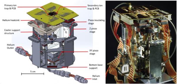
Figure 5: (Left) 3D drawing of the cryogenic support structure used to ensure both mechanical stability and thermal insulation. The PCBs (gold) are used to deliver electric signal to the trap for ion confinement, shuttling and entanglement purposes. (Right) Assembled setup including DC and RF cables for signal delivery to the PCB.
To deliver the cooling power, a remote cryogenic station uses a combination of two single-stage cryocoolers to refrigerate the helium gas. Gaseous helium is then circulated to the experiment along transfer lines by means of a centrifugal pump. Heat being dissipated at the ion trap setup is then captured by the gaseous coolant at the heat sink location and is then recirculated to the cryostat station, the circulation process is described in Figure 6.
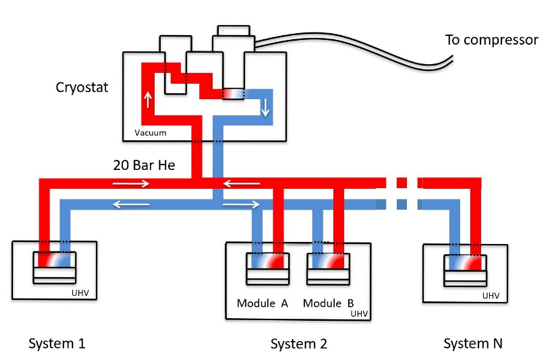
Figure 6: Schematics of the close-loop helium circulating cryostat used to deliver cooling power to multiple ion trapping modules or experiments.
In a drastic shift from other cryogenic ion trapping experiments around the world, and to remain entirely focused toward scalability, this cryogenic cooling scheme is limited by neither the footprint nor cooling power of commercially available cryocooler. Indeed, by physically decoupling both ion trapping apparatus from cryostat, this closed-loop cryogenic cooling architecture inherently ensures modularity while matching the cooling requirement of high-power devices. To demonstrate the cryostystem’s intrinsinc scalability, we use this setup to deliver cooling power to four ion trapping experiments simultaneously across the laboratory, a picture of the cryostat delivering the cooling power to all four experiment is shown in Figure 7.
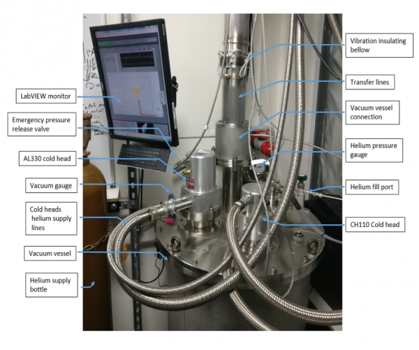
Figure 7: Picture of the cryostat which has been constructed in the laboratory and currently deliver cooling power to four ion trapping setups.