Ion microchips form the core of quantum computers, quantum simulators and quantum sensors with trapped ions. We run a comprehensive development program for such devices in our group. Work is carried out at numerous clean room facility as well as industrial foundries along with a small clean room facility we host in our group at Sussex.
We provide an overview of state-of-the-art microfabrication techniques, as well as various considerations which motivate the choice of materials and processes in reference [1] where we also discuss current efforts to include advanced, on-chip features into next generation ion traps. An earlier review paper from our group discusses the basics of ion trapping and provides a good overview of the different fabrication methods [2].
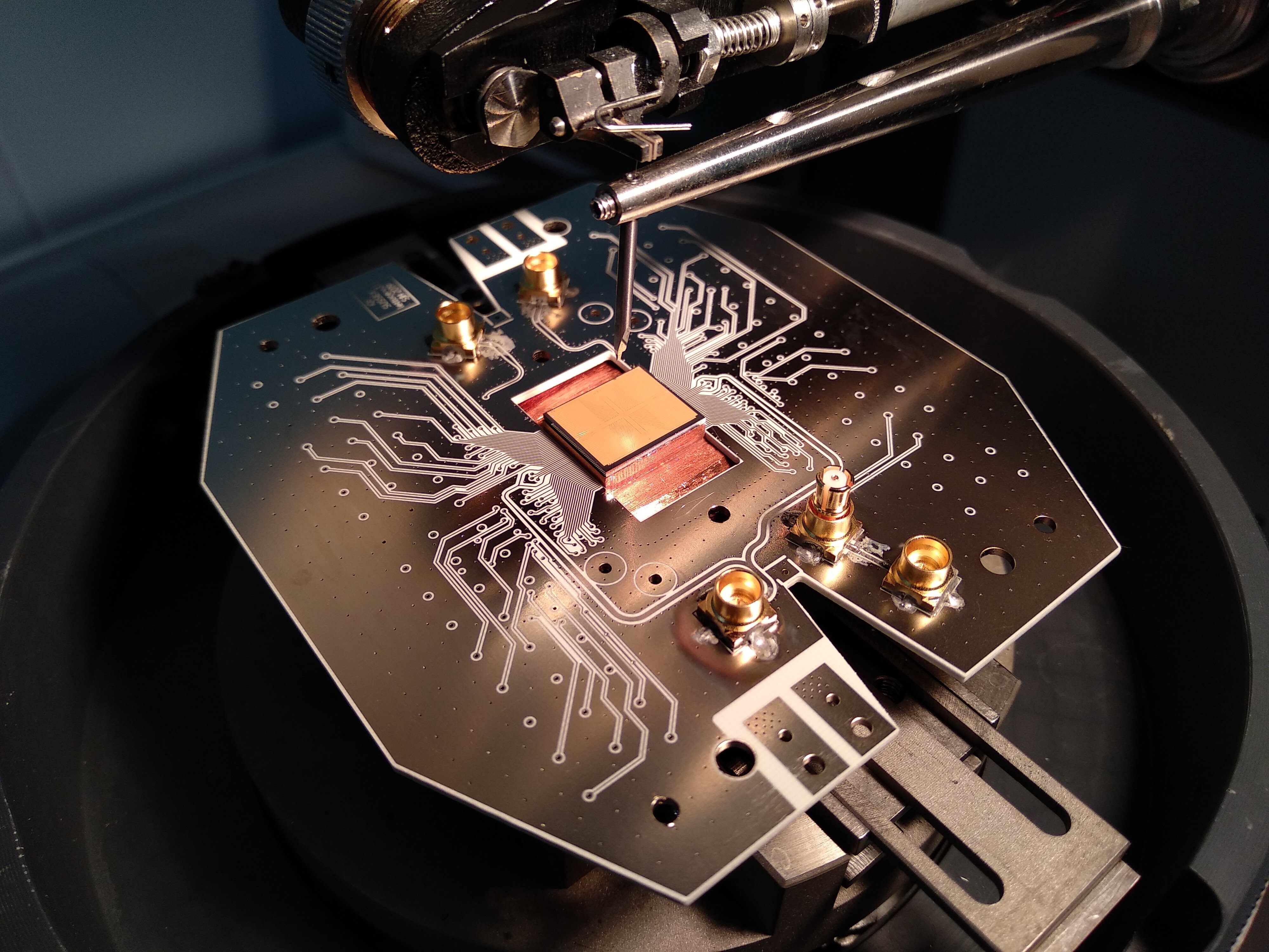
We published the first blueprint on how to build a practical quantum computer [3]. This blueprint contains the idea of fully electronic quantum computing modules. In order to develop such modules (shown in Fig. 1), we need to integrate additional features such as digital to analogue converters, FGPA, and detectors.
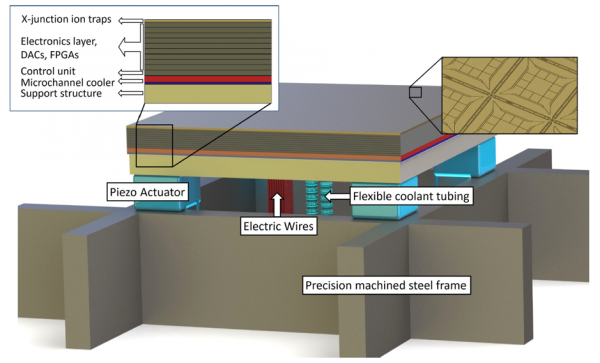
Figure 1: Illustration of an electronic quantum computing module
To achieve complex electrode geometries (for example segmented inner electrodes completely surrounded by others) we fabricate ‘buried wires’, which are thin layers of metal that are placed underneath the trap structure to allow the inner electrodes to be electrically connected to pads on the outside of the chip. Furthermore, our quantum computing approach requires the presence of strong magnetic field gradients. These are generated using current-carrying wires formed by copper tracks beneath the trap electrodes to generate extremely high magnetic field gradients.
The structure of such an ion chip as shown in Fig. 2.
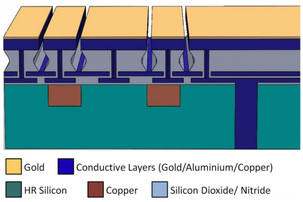
Figure 2: Cross section of an ion trap microchip with integrated current carrying wires and VIAs for backside connections.
X-junction ion trap chips as shown in Fig. 3 form a typical ion trap geometry. A magnetic field gradient in one of the linear trapping regions allows for an ‘entanglement region’, and other arms of the junction can be designated as ion loading and detection regions.
Figure 3: Electron microscope image the X junction trap electrodes. Microchip developed in collaboration with the University of Southampton
This trap forms the basic building block for a fully scalable ion trap quantum computer, made up of an array of X junction traps that join to form a 2D grid of ion traps that can be extended to an arbitrarily large size. Algorithms could then be performed on the chips, by combining multi-qubit operations and shuttling of ions through the junctions.
Combining the dedicated entanglement, trapping and detection regions of these chips with sheets of laser cooling light and on-chip features such as photodetectors, and digital-to-analog converters allows for large numbers of ions to be used in a scalable architecture for quantum information processing.
Other advanced features of our microchips include slots fabricated in the trap structure that pass through the entire substrate, for the alignment of atomic beams and detection of ion fluorescence. A chip we have fabricated featuring an optical access hole is shown in Figure 4.
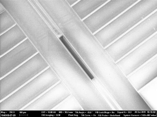
Figure 4: Ion microchip with optical access hole.
In order to realize a fully electronic quantum computing module, further chip layers need to be developed that are bonded to the ion chip to add relevant electronics to give rise to a structure as shown in Fig. 5.
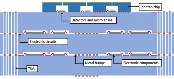
Figure 5: Additional chip layers that are bonded to the ion chip to give rise to an electronic quantum computing module
For large trap depths and consequently long ion lifetimes and low heating rates, it is important to be able to apply large voltages to microfabricated ion traps. The voltages that can be applied are limited by the breakdown voltage of the chip – this is the voltage at which discharge between adjacent electrodes occurs in the form of a flashover.
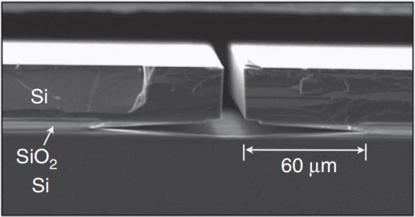
Figure 6: Deep V-shaped undercut in dielectric layer, shown in cross section. Microchip developed in collaboration with the University of Southampton
We have demonstrated a new technique to allow for the application of very high voltages to microfabricated ion traps. By etching a large V-shaped undercut in the dielectric layer (figure 6), the path length between the trap electrodes and the ground plane is drastically increased, which in turn results in very high breakdown voltages [4].
Another method of increasing the breakdown voltage of microfabricated ion traps which has been developed by our group involves modifying the fabrication process and the use of specialized dielectric materials [5]. By using this method, the breakdown voltage for both dc and RF was more than doubled when compared to previous microchips. This result has a significant impact on the realization of next-generation micro- and nano-fabricated devices and for the fabrication of ion trapping arrays for the realization of scalable ion quantum technology.
Our group has extensive experience in the development of microchips for different purposes.
A 2D lattice of trapped ions opens up the possibility of experiments that are difficult or impossible to perform using linear RF traps. These potential applications include spatial magnetic and electric field sensing [6-8] , force detection [9], interactions between neutral atoms and ions [10] and cluster state quantum computing [11]. On top of this, it might be possible to perform analogue quantum simulations, where the Hamiltonian of a complicated many-body system can be realized and its properties measured [12, 13].
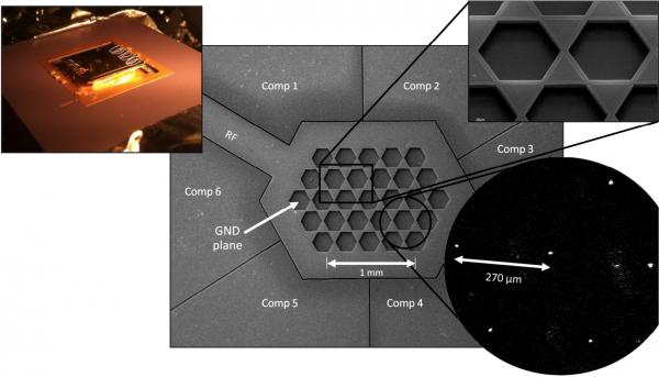
Figure 7: 2D array ion trap, showing electrode structure and lattice of trapped ions. Microchip developed in collaboration with the University of Southampton
We have already demonstrated the design, fabrication and successful operation of a 2D hexagonal array ion trap microchip which has been published in Nature Communications in April 2014 [4]. This constituted the first 2D ion lattice on a microchip (figure 7); an architecture capable of scaling to a very large number of ions. Not only can this architecture be used to reduce the ion-ion spacing sufficiently to be used for quantum simulation, it also has significant applications in the field of metrology and magnetic field sensing.
The trap was fabricated using a silicon-on-insulator wafer, with the recessed plane being used as a common ground electrode, and the raised surface as the radio-frequency (RF) electrodes. By etching a deep V-shaped undercut between the electrodes, extremely high breakdown voltages have been achieved with these chips: 1298(5) V for dc and 1061(32) V for RF.
Ions are reliably trapped in each of the lattice sites, and ‘lattice defects’ introduced by either leaving a trapping site vacant, or by trapping multiple ions in one site which is an additional important capability for the implementation of quantum simulations. We have also demonstrated shuttling operations between sites by lowering the applied RF voltage to reduce the potential barrier between sites, then varying the voltages applied to the six dc control electrodes, placed around the RF electrode.
Having demonstrated a scalable architecture for 2D quantum simulation we have also developed a method for determining the optimum geometry of the lattice which is capable of achieving the largest possible ratio of the interaction rate between the ions and various sources of decoherence [16].
This work in conjunction with our previous work on 2D arrays has led to the development of our new generation of 2D array microchips (figure 8).
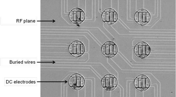
Figure 8: Electron microscope image of the 2D square array trap electrodes. Microchip developed in collaboration with the University of Southampton
These novel microchips which are the first of its kind consist of 9 trapping sites. Each trapping site has dc electrodes to move each ion independently, allowing for individual micromotion compensation. There are three versions of this trap, with ion separations of 52 µm, 85 µm and 185 µm, which may allow for sufficient nearest neighbour coupling between the ions via their mutual Coulomb interaction capable for use in quantum simulation experiments.
We have developed ion trap chips with other functionalities. Figure 9 shows a vertical shuttling traps with integrated high Q microwave resonator. This vertical shuttling trap uses RF electrodes of varying width to change the ion-electrode distance as the ions are shuttled along the trapping region. These traps allow for measurement of ion heating rates at a number of different ion heights in the same experiment, and also include an integrated high-Q microwave cavity. This allows us to trap ions and detect their fluorescence at a large ion height, and bring them to a lower ion height to interact with the microwave fields, benefitting from both low heating rates and strong ion-microwave field coupling.
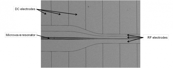
Figure 9: Electron microscope image of the vertical shuttling and microwave cavity trap electrodes. Microchip developed in collaboration with the University of Southampton
An ion trap with a closed circular trapping region allows for new types of experiments to be performed using trapped ions that are not possible with linear or lattice geometries, by storing an ion string with uniform ion separation and observation ion-ion interactions with periodic boundary conditions. Potential applications of this trap include investigating the homogenous Kibble-Zurek mechanism [17], Hawking radiation [18] and space time crystals [19].
In 2013, the IQT group demonstrated the successful operation of a ring trap microchip (figure 10), which has one continuous, circular trapping region above which a string of ions can be confined. The ring trap has a radius of 1690 µm and ion-electrode distance of 245 µm, and secular frequencies of 720 kHz (radial) and 210 kHz (axial) and trap depth of 0.1 eV with an RF voltage of 190 V.
The trap was created using advanced microfabrication techniques, which allow for the electrical connection of central segmented electrodes to the outside of the microchip using buried wires under the electrode geometry and vertical interconnects. The trap electrodes consist of a very thick (15 µm) electroplated gold layer, with layered Si02 and Si3N4 dielectrics on a quartz wafer.
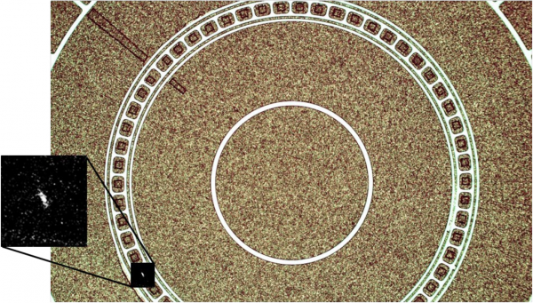
Figure 10: Microscope image of the ring trap surface, and image of an ion trapped above the surface. Microchip developed in collaboration with the University of Nottingham
Another ion trap microchip we have realized is a flat multipole ion trap chip. The flat multipole trap could be used to trap multiple ion strings in adjacent linear trapping regions, such that a large number of ions can be trapped in the same plane. This structure of trapped ion crystals has possible applications in new types of quantum simulations that can be performed.
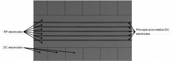
Figure 10: Electron microscope image of the flat multipole trap electrodes. Microchip developed in collaboration with the University of Southampton
References
[1] Zak David Romaszko, Seokjun Hong, Martin Siegele, Reuben Kahan Puddy, Foni Raphaël Lebrun-Gallagher, Sebastian Weidt and Winfried Karl Hensinger, Engineering of Microfabricated Ion Traps and Integration of Advanced On-Chip Features, arXiv:1908.00267 [physics.app-ph] (2019)
[2] Marcus D. Hughes, Bjoern Lekitsch, Jiddu A. Broersma and Winfried K. Hensinger, Microfabricated Ion Traps, Contemporary Physics 52, 505 (2011), pdf
[3] B. Lekitsch, S. Weidt, A.G. Fowler, K. Mølmer, S.J. Devitt, Ch. Wunderlich, and W.K. Hensinger, Blueprint for a microwave trapped ion quantum computer, Science Advances 3, e1601540 (2017)
[4] R. C. Sterling et al, Fabrication and operation of a two-dimensional ion-trap lattice on a high-voltage microchip. Nature Communications 5, 3637 (2014)
[5] R. C. Sterling et al, Increased surface flashover voltage in microfabricated devices. Appl. Phys. Lett. 103, 143504 (2013)
[6] S. Kotler et al, Single-ion quantum lock-in amplifier. Nature 473, 61–65 (2011)
[7] S. Narayanan et al, Electric field compensation and sensing with a single ion in a planar trap. J. Appl. Phys. 110, 114909 (2011)
[8] M. Brownnutt et al, Spatially-resolved potential measurement with ion crystals. Appl. Phys. B 107, 1125–1130 (2012)
[9] M. J. Biercuk et al, Ultrasensitive detection of force and displacement using trapped ions. Nat. Nanotechnol. 5, 646–650 (2010)
[10] C. Zipkes et al, A trapped single ion inside a Bose-Einstein condensate. Nature 464, 388–391 (2010)
[11] R. Raussendorf & H. J. Briegel, A one-way quantum computer. Phys. Rev. Lett. 86, 5188–5191 (2001)
[12] C. Schneider, D. Porras & T. Schaetz, Experimental quantum simulations of many-body physics with trapped ions. Rep. Prog. Phys. 75, 024401 (2012)
[13] R. Blatt & C. F. Roos, Quantum simulations with trapped ions. Nat. Phys. 8, 277–284 (2012)
[14] M. Kumph, M. Brownnutt & R. Blatt, Two-dimensional arrays of radiofrequency ion traps with addressable interactions. New J. Phys. 13, 073043 (2011)
[15] R. J. Clark et al, A two-dimensional lattice ion trap for quantum simulation. J. Appl. Phys. 105, 013114 (2009)
[16] J. D. Siverns et al, Optimisation of two-dimensional ion trap arrays for quantum simulation, New J. Phys. 14, 085009 (2012)
[17] S. Fishman et al, Structural phase transitions in low-dimensional ion crystals. Phys. Rev. B 77, 064111 (2008)
[18] T. Li et al, Space-Time Crystals of Trapped Ions. Phys. Rev. Lett. 109, 163001 (2012)
[19] B. Horstmann et al, Hawking Radiation from an Acoustic Black Hole on an Ion Ring. Phys. Rev. Lett. 104, 250403 (2010)