Engineering and interdisciplinary technology development
Dr Richard Feynman said that building a quantum computer “doesn’t look so easy”. Perhaps he was thinking of only the quantum aspects of the computer. But this extends into the engineering – to the electronics. Circuits need to be designed that can control these delicate quantum processes.
As electronic engineers embedded in the group, we focus on design challenges coming from all directions;
- The environment is hostile – ultra-high vacuum, cryogenic temperatures,
- The requirements can be contradictory – ultra-stable and ultra-low-noise, but fast too.
- The data flow rates are high – thousands of synchronous DAC updates per µ
- The manufacturing is difficult – dense circuitry, spanning large areas.
But we are facing-up to the challenge. Three dimensional wafer scale electronic systems using cutting edge assembly technology are needed. Distributed digital processing, distributed memory, distributed DACs, they all need to be acting together using a custom system architecture that spans the entire silicon wafer. Exotic components need to be integrated; Single Photon Avalanche diodes (SPAD), atomic ovens. All of this is being explored by the group’s engineering team.
The work we do is pushing the boundaries of available technology
Until recently, workbench (PCB) based electronics have been adequate to support the quantum-gate developments. We operate commercially available equipment but we are not afraid to develop our own when the performance is just not good enough. These include ultra-stable (5ppm) current sources and arrays of ultra-stable voltage sources. We verify the designs using the best measurement procedures and equipment, but PCB based electronics cannot be used to build a scalable quantum computer.
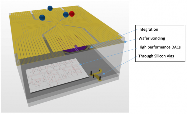
Whilst continuing to support quantum gate development, and using what we have learnt from the experiments, we are now actively researching the specification and design of a wafer sized electronic system. This Application Specific Integrated Circuit (ASIC) is likely to require cutting edge assembly processes to integrate with the quantum processing gates, not least through silicon vias (TSV) and wafer bonding but also assemblies that can withstanding the extreme environment in which the system operates.
Challenges squared
Not only is the technology we are designing with at the forefront of today’s electronic design processes, it is as much of a challenge to integrate all of it in a high density scale-able design. We don’t just need to get a technology working, we need to optimise it for performance, power, size and interoperability. That’s why the work we do is relevant to applications across all technological industries, from space exploration (low temperature electronics), portable medical equipment (low noise, high accuracy), right through to mobile phones and device miniaturisation (3D circuits, power efficiency).
Reliability and manufacturability are also key to the success of the project, due to the enormous size of the first quantum computer and the necessity of large area electronics on the wafer scale. This means that even though we are designing with near-future technologies, we need to design them with mass production in mind and achieve extremely high yields for such an early adoption – paving the way for these technologies to become common place in every electronic designer’s tool kit.
Spad picture taken from:
https://www.eenewseurope.com/news/x-fab-now-offering-spad-and-apd-devices-180nm-process)